In compliance with EU personal data protection laws, we are committed to protecting your personal data.
By clicking "Accept All", you allow us to place cookies to enhance your experience on this site, help us analyze site performance and usage, and enable us to deliver relevant marketing content. You can manage your cookie settings below. By clicking "Accept All" you agree to the current settings.
1-1. Please measure the signal output by two terminals of the crystal using Oscilloscope or Frequency Counter. If there is no signal output, please follow step 1-1 to step 1-4 to execute the examination. If there is signal output from out- terminal of the crystal ( Xout), but no signal output from the in-terminal (Xin), please check the crystal following step1-5 to step 1-6.
1-2. Please uninstall the crystal and test its frequency and load capacitance to see whether they vibrate and meet your specifications using a professional testing machine. You can also send it to your supplier to have them test it for you.
1-3. If any of the following situations happen, the crystal doesn’t vibrate, its load capacitance doesn’t match your specification, or there is a huge gap between current frequency and your targeted frequency, please send the crystal to your supplier to conduct Quality Analysis. If the frequency and load capacitance meet your specifications, we will need to conduct Equivalent Circuit Test.
1-4. Equivalent Circuit Test
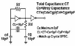
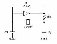
1-4-1. Generally, the oscillation circuit of Microprocessor derives from Colpitts circuit showing above: Cd and Cg are external load capacitances, which have been built in the chip set. (Please refer to the Specifications of the chip set)
Rf is the feedback resistance with200KΩ~1MΩ. It’s built in the chip set generally.
Rd is the Limit Resistor with 470Ω~1KΩ. This resistance is not necessary for common circuit but only for circuits having high power supply.
1-4-2. A stable oscillation circuit requires a negative resistance and its value should be at least five times of the crystal resistance. It can be written as |-R| > 5 Rr. For example, to acquire a stable oscillation circuit, the value of negative resistance of the IC must be under –200Ω when the value of the crystal resistance is 40Ω.
1-4-3. “Negative resistance” is the yardstick to evaluate the quality of an oscillation circuit. Under some circumstances such as aging, thermal change, voltage change, and etc., the circuit might not oscillate if the value of “ Q” is low. Thus, it’s very important to measure the negative resistance (-R )following the instructions below:
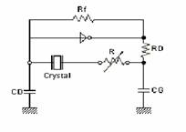
- Connect the resistance (R) with the crystal in series
- Adjust the value of R from the start point to the stop point of the oscillation.
- Measure the value of R during oscillating.
- You will be able to obtain the value of negative resistance, |–R| = R + Rr, and Rr = crystal resistance.
P.S. the stray capacitance of the connected circuit might affect measured values.
1-4-4. If the parameters of the crystal are normal but it’s not working steadily within the oscillation circuit, we will have to find out whether the resistance value of the IC is too low to drive the circuit. If that’s the case, we have three methods to improve such situation:
- Lower the value of external capacitance(Cd and Cg), and adopt other crystal with lower load capacitance (CL).
- Adopt a crystal with lower resistance (Rr).
- Measure the value of R during oscillating.
Using the design of unequal values of Cd and Cg. We can increase the load capacitance of Cd (Xout) and decrease the load capacitance of Cg(Xin) to raise the output of waveform amplitude from Xin which will be used in its back-end circuit.
1-5. When there is signal output from Xout but not Xin, it represents the case that the power consumption of the rear - electrode Backend Circuit is extremely huge. We can add a buffer between the output of the circuit and its rear electrode to drive the back-end Circuit.
1-6. Except the method of 1-5 mentioned above, you can also follow the three methods in step 1-4-4. Please contact the field application engineers of crystal or IC manufacturers for further assistance, if your problem can’t be solved.
2-1. Please measure the signals from the two terminals of the crystal using Oscilloscope or Frequency Counter, if the Frequency is not within the specification and it’s output waveform amplitude is not adequate (for example, over+/- 200ppm), please follow step 2-3 to step 2-5.
2-2. The formula for Capacitances versus Frequency is as following:  FL = FR * ( 1 + C1 / 2 * ( C0 + CL) ) where
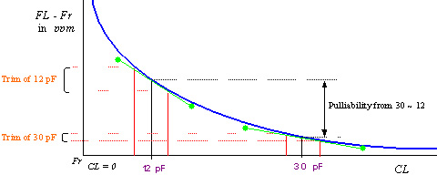
The curve represents the variation of capacitance changes versus variation of frequency changes ( Frequency pullability):
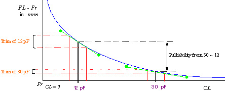
If the frequency measured by Frequency Counter is higher than the targeted frequency, we should increase the value of capacitances (CL, or Cd & Cg ) to lower the frequency to the targeted frequency, vice versa.
Please check whether the waveform amplitude is improved or not after we adjust the frequency. If it’s improved, that indicates the case that the original design of the circuit is not tuned to the best resonant point for the crystal. The crystal should function normally after the resonant point is adjusted.
2-3. If the waveform amplitude is not improved even the frequency is pretty much close to the targeted frequency, we can improve it using three methods below:
Method 1: Lower the value of external capacitance (Cd, and Cg) , and adopt crystal with lower load apacitance (CL).
Method 2: Adopt the crystal with lower resistance(Rr).
Method 3: Use the design of unequal values of Cd and Cg.
We can increase the load capacitance of Cd (Xout) and decrease the load capacitance of Cg(Xin) to raise the output of waveform amplitude from Xin which will be used in its back-end Circuit.
We suggest that you use above methods to save costs and assure safety.
2-4. Please use the Frequency Counter to measuring the crystal to ensure that the adjusted frequency still meets original specification after the waveform amplitude has been improved. If the frequency doesn’t meet the specification, please adopt a crystal with suitable CL value according to your targeted frequency.
2-5. Please adopt a crystal with lower CL if the frequency is much higher than the targeted frequency, vice versa.
3-1. We can improve the problem that deviation of frequency output is over the limit by following methods:
Method 1: Adjust the values of external capacitance, Cd & Cg. If the frequency measured by Frequency Counter is higher than targeted frequency, we should increase the external capacitance, CL ( or the values of Cd & Cg ), to lower the frequency to our targeted frequency, vice versa.
Method 2: Adopt a crystal with different value of capacitance(CL). Adopt a crystal with lower capacitance if the frequency is much higher than the targeted frequency, vice versa.
3-2. Please check whether the waveform amplitude is normal or not using Oscilloscope, after the correct capacitance is adopted and the frequency is adjusted to target. Under the situation that the waveform amplitude is shrunk due to adding external capacitances, please use method 2 to adjust the frequency ( lower external capacitances and adopt a crystal with lower capacitance).
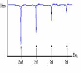
4-1. The curve below represents the characteristics of the resistance of a crystal:

A crystal has various vibration modes such as Fundamental, 3rd overtone, 5th overtone,….and etc.. When the fundamental mode is applied, the resistance of the crystal is lowest, which means it’s easiest for the crystal to oscillate. When the third-tone mode is applied, a magnifying circuit must be utilized to lower the frequency feedback of fundamental mode to the extend less than the third tone mode. Therefore, if the frequency is only one third of the targeted frequency, we should check whether magnifying circuit is applied or its setting value is adequate since the circuit environment is suitable for fundamental mode instead of third-tone mode.
4-2. The circuit might not oscillate if the magnifying circuit is not applied or its setting value is not adequate.
4-3. The applications of Fundamental mode and Third-Tone mode are as following:
a. Application of Fundamental mode
b. Application of Third-Tone mode
4-4. The table below shows the match values of L, C for Third-Tone mode by various frequency:

5-1. The chances of this problem are relatively small. Please identify whether the frequency feedback of third-tone mode is larger than the feedback of fundamental mode due to magnifying circuit. This problem might happen when the magnifying circuit is built in the chip set. To solve this problem, please adopt third-tone mode crystal.
5-2. Furthermore, inappropriate design of magnifying circuit for third-tone mode might also cause the circuit to oscillate by fifth-tone mode or fail to oscillate.
6-1. Please refer to solution of situation 2. Please increase the capacitance of terminal Xin, and then check whether waveform amplitude is improved.
7-1. Please identify the frequencies of interrupting signals using Spectrum Analyzer machine. We can find out what the problems are according to the frequencies.
7-2. If it’s AC signal from power supply, please check whether the status of both grounds of power supply and signal is floating. Please change to floating if it’s not.
7-3. If the signal has high frequency, please use the methods below:
- Use the shell of crystal as the ground.
- Adopt a crystal with smaller C0 .
- Increase external capacitance of the circuit, Cd & Cg, and adopt a crystal with higher load capacitance,CL.
7-4. Please check surrounding circuits and the PCB layout, if the methods above are not able to solve your problem. If both of them are normal, please ask IC manufacturer to investigate the reaction of its chip set design to unknown signals. Changing the design of surrounding circuit can only alleviate the problem instead of totally solve it. Usually. It will be the best to find out the problem of the chip set design and solve it.
The solutions for this problem is as the same as problem 7. Please refer to step 7-1 to step 7-4 .
9-1. Please use Oscilloscope or Frequency Counter to measure the signals from the two terminals of the crystal. Please follow step 9-1 to 9-4 to test. When there is signal output from Xin but its waveform amplitude is small, please follow step 2-1~2-5 to test.
9-2. Please uninstall the crystal and test its frequency and load capacitance to see whether they vibrate and meet your specifications using a professional testing machine. You can also send it to your supplier to have them test it for you.
9-3. If any of the following situations happen, such as, the crystal doesn’t vibrate, its load capacitance doesn’t match your specification, or there is a huge gap between current frequency and your targeted frequency, please send the crystal to your supplier to conduct Quality Analysis.
9-4. If the frequency and load capacitance meet your specifications and the crystal pass DLD test, we will need to conduct Equivalent Circuit Test. Please refer to step 1-4 ~ 1-6.
9-5. If the crystal fails the DLD test , please send it to your supplier to conduct Quality Analysis for further improvement.
10-1. Uninstall the crystal and test its frequency and resistance to see if it oscillate and meets the specifications using thermal testing machine. You can also send it to the crystal supplier to test. ( The thermal test points should have the interval of at least 10℃/1 test point)
10-2. Please send the crystal to the manufacturer for Quality Analysis and further improvement, if its resistance and frequency is out of the specifications within working temperature.
10-3. In the case of the crystal passes the thermal test, please check the oscillation circuit and the characteristics of other components such as its temperature characteristic of external capacitance,temperature characteristic of chip circuit, and etc.. ).
11-1. As shown below, there is negative correlation between the capacitance of the VCXO circuit and pullability, which means when the capacitance gets smaller, the frequency pulling range(FL-Fr) gets larger, vice versa. /since the capacitance of the VCXO circuit is controlled by Varistor, we can enlarge the frequency pulling range by using Varisitor with smaller capacitance or wider adjusting range.
11-2. Except external circuit adjustment, the characteristic of crystal parameter also affects frequency pulling range. Its reference parameters are Trim Sensitivity(TS), C0/C1(r), C1,C0 and etc.. The relationships among each paramenter and frequency pullability are as following:
C0↑ , C1↑, C0/C1(r)↓ , TS↑ , pullability ↑
11-3. If the frequency pulling rang is not adequate, we can also adjust the specification of the crystal to meet targeted range.
11-4. When the pulling of one side is not enough and the other side is too large due to the pulling range is asymmetric, we can adjust the load capacitance (CL)of the crystal to reach symmetry and enough pulling for both sides.
12-1. According to the curve of crystal pull ability shown at 11-1, the smaller the capacitance gets, the larger the effect on Frequency change. Please follow the methods below if the distribution of the frequency is too wide:
- Increase the value of capacitances, Cd and Cg, and adopt a crystal with larger load capacitance (CL).
- Use more sophisticated capacitance for Cd & Cg (Capacitance varies little).
- Use more sophisticated crystal (Frequency varies little).
12-2. Furthermore, if the distribution of the frequency can’t be improved to meet the specifications due to the stray capacitance of PCB is relatively large , it might require a new layout based on the sources of stray capacitance.

